

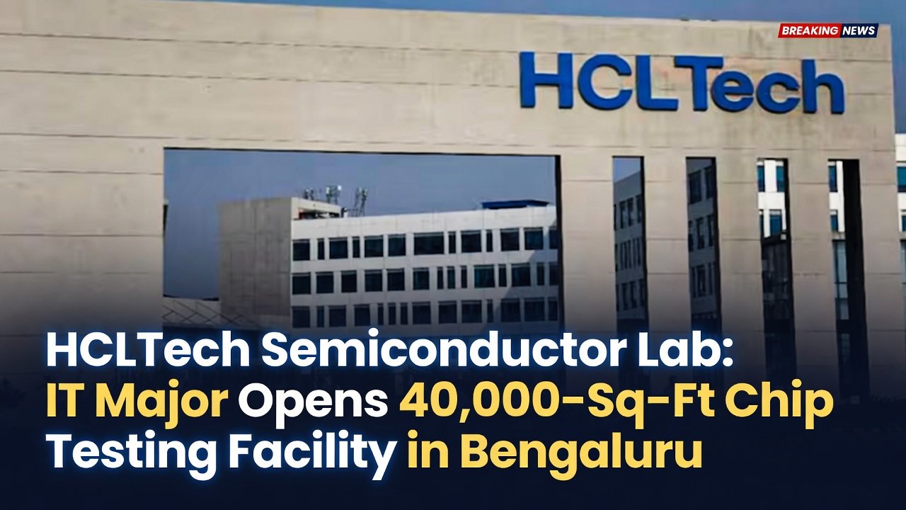
HCLTech Semiconductor Lab: IT Major Opens 40,000-Sq-Ft Chip Testing Facility in Bengaluru
The HCLTech Semiconductor Lab has officially opened in Bengaluru as the IT major expands its presence in India’s rapidly developing semiconductor ecosystem.
The new facility covers approximately 40,000 square feet and has been established with an investment of ₹185 crore. The state-of-the-art laboratory will focus primarily on semiconductor testing and validation, supporting the development and verification of advanced chip technologies.
The launch represents another significant step in HCLTech’s strategy to strengthen its semiconductor engineering capabilities while contributing to India’s broader ambitions of developing a stronger domestic chip ecosystem.
HCLTech Opens New Semiconductor Facility
HCLTech has established the new semiconductor laboratory in Bengaluru, one of India’s most important technology and engineering hubs.
The facility has been designed specifically to support semiconductor testing and validation activities. These processes are essential for ensuring that chips perform according to their intended specifications before they move toward commercial deployment.
With the ₹185 crore investment, HCLTech is expanding its physical infrastructure at a time when semiconductor technology is becoming increasingly important across industries.
40,000-Sq-Ft Facility in Bengaluru
The new HCLTech Semiconductor Lab spans around 40,000 square feet.
The facility has been developed as a specialized environment for semiconductor engineering and testing rather than as a conventional IT office.
Its infrastructure is expected to support engineers and technology teams working on chip validation, testing and related semiconductor development activities.
Bengaluru’s established engineering talent pool and technology ecosystem make the city a natural location for such an advanced facility.
Focus on Chip Testing and Validation
The primary purpose of the laboratory is chip testing and validation.
Semiconductor testing is a critical stage in the chip development process. Before a semiconductor product can be deployed at scale, engineers need to verify its functionality, performance and reliability.
Validation can involve testing chips under different operating conditions and checking whether they meet technical specifications.
For technology companies, strong testing capabilities can help identify design or performance issues before products reach customers.
The new laboratory is therefore expected to play an important role in HCLTech’s semiconductor engineering operations.
Why Semiconductor Testing Matters
Modern electronic devices depend on increasingly sophisticated semiconductor components.
Smartphones, automobiles, data centres, telecommunications equipment, artificial intelligence systems and industrial machinery all require advanced chips.
As chip designs become more complex, testing and validation become equally important.
A semiconductor may function correctly under normal conditions but encounter problems under higher temperatures, heavier workloads or different voltage conditions. Testing laboratories allow engineers to identify such issues and improve product reliability.
HCLTech’s investment in dedicated testing infrastructure reflects the growing importance of this stage of semiconductor development.
Bengaluru Strengthens Its Semiconductor Position
Bengaluru has long been known as India’s technology and engineering capital.
The city hosts a large concentration of software companies, engineering teams, research institutions and global technology centres.
Its semiconductor ecosystem has also expanded as companies increasingly establish chip-design and engineering operations in the city.
The new HCLTech facility adds another specialized semiconductor capability to Bengaluru’s technology landscape.
₹185 Crore Investment Signals Long-Term Commitment
The ₹185 crore investment represents a substantial commitment to semiconductor engineering infrastructure.
Rather than relying entirely on existing facilities, HCLTech is creating a dedicated laboratory designed around the specific requirements of chip testing and validation.
Such investment can help companies develop deeper technical expertise and provide customers with more specialized semiconductor engineering services.
It also reflects the increasing commercial importance of semiconductor-related services within the broader technology industry.
HCLTech Expands Beyond Traditional IT Services
HCLTech is traditionally known for IT services, digital transformation and technology consulting.
However, the company’s semiconductor activities represent a broader expansion into engineering-led technology services.
Semiconductor engineering requires specialized knowledge spanning chip architecture, design, verification, validation, testing and system integration.
By investing in dedicated infrastructure, HCLTech can strengthen its ability to support customers throughout more stages of the semiconductor development cycle.
Supporting India’s Semiconductor Ambitions
The launch comes as India is attempting to build a stronger semiconductor ecosystem.
The country has traditionally been a major hub for semiconductor design and engineering talent, while much of the world’s large-scale chip manufacturing has remained concentrated in other regions.
Government incentives and investments from global and domestic companies are now aimed at expanding India’s capabilities across semiconductor manufacturing, packaging, testing and design.
Facilities such as the HCLTech laboratory can contribute to this ecosystem by strengthening the engineering and testing capabilities available within India.
Growing Demand for Chip Engineering
The global demand for semiconductors continues to expand as more products become digitally connected.
Artificial intelligence is creating additional demand for high-performance computing chips, while electric vehicles require increasingly sophisticated semiconductor systems.
At the same time, industries such as telecommunications, healthcare, defence and consumer electronics continue to depend heavily on advanced semiconductor technology.
This growth is creating opportunities not only for chip manufacturers but also for companies providing design, testing, validation and engineering services.
Role of Testing in the Semiconductor Supply Chain
Semiconductor development involves several stages.
The process typically begins with architecture and chip design, followed by verification, fabrication and testing. Once chips are manufactured, engineers need to confirm that the final products meet their intended specifications.
Testing can identify manufacturing defects, performance issues and reliability problems.
Validation also helps ensure that a chip works correctly when integrated into the larger system for which it was designed.
The new HCLTech facility is focused on this crucial portion of the semiconductor value chain.
Potential Benefits for HCLTech Customers
A dedicated semiconductor testing facility can provide customers with access to specialized engineering infrastructure.
Companies developing semiconductor products may require testing support at different stages of development, particularly as chip designs become more sophisticated.
By offering testing and validation capabilities from Bengaluru, HCLTech can potentially provide customers with faster engineering cycles and access to India’s large pool of technical talent.
The facility could therefore become an important component of the company’s semiconductor services strategy.
Bengaluru’s Engineering Talent Remains a Key Advantage
One of India’s biggest advantages in semiconductor engineering is its large pool of skilled engineers.
Bengaluru has developed deep expertise in chip design, embedded systems, electronics and software engineering over several decades.
This talent base has attracted semiconductor companies from around the world.
For HCLTech, locating its new semiconductor laboratory in Bengaluru provides access to an ecosystem already familiar with advanced engineering and technology development.
India’s Semiconductor Ecosystem Continues to Evolve
The establishment of the HCLTech Semiconductor Lab is part of a larger transformation taking place within India’s semiconductor industry.
India is increasingly seeking to move beyond its traditional role as a semiconductor design and software engineering centre.
New investments are targeting chip fabrication, assembly, testing and packaging, while established technology companies are expanding their semiconductor engineering capabilities.
The combination of manufacturing infrastructure and engineering expertise could help India become a more important part of global semiconductor supply chains.
What Happens Next?
The Bengaluru laboratory is expected to support HCLTech’s semiconductor engineering activities as the company expands its capabilities in testing and validation.
Future developments could include additional investments, technology partnerships and expansion of semiconductor-related services.
As demand for chip engineering continues to grow, specialized facilities could become increasingly important for technology companies seeking to compete in the global semiconductor market.
Why the HCLTech Semiconductor Lab Matters
The new facility represents more than an expansion of office space.
The HCLTech Semiconductor Lab gives the company dedicated infrastructure for a highly specialized part of the chip development process.
With a ₹185 crore investment and a 40,000-square-foot facility, HCLTech is signalling a long-term commitment to semiconductor engineering in India.
For Bengaluru, the facility further strengthens the city’s position as a major global centre for advanced technology and chip-related engineering.
Key Takeaway
The HCLTech Semiconductor Lab has opened in Bengaluru following an investment of ₹185 crore by HCLTech.
The 40,000-square-foot facility will focus on semiconductor testing and validation, providing specialized infrastructure for engineers working on advanced chip technologies.
The launch comes as India’s semiconductor ecosystem continues to expand, with companies investing in design, manufacturing, testing and engineering capabilities.
For HCLTech, the facility strengthens its semiconductor services portfolio, while for Bengaluru, it adds another major investment to the city’s growing position as a hub for semiconductor and advanced technology engineering.
FAQs
1. What is the HCLTech Semiconductor Lab?
The HCLTech Semiconductor Lab is a new 40,000-square-foot semiconductor engineering facility in Bengaluru focused on chip testing and validation.
2. How much did HCLTech invest in the facility?
HCLTech invested ₹185 crore in establishing the new semiconductor laboratory.
3. Where is the HCLTech Semiconductor Lab located?
The facility is located in Bengaluru, Karnataka.
4. What will the facility focus on?
The laboratory will primarily focus on semiconductor testing and validation.
5. Why is semiconductor testing important?
Testing and validation help engineers verify chip performance, reliability and functionality before semiconductor products are deployed commercially.
6. Why did HCLTech choose Bengaluru?
Bengaluru has a large technology and engineering talent pool and an established ecosystem for semiconductor design and advanced technology development.
7. Does HCLTech manufacture semiconductor chips?
The new facility is focused on testing and validation, rather than being described as a semiconductor manufacturing plant.
8. How big is the new laboratory?
The HCLTech Semiconductor Lab covers approximately 40,000 square feet.
9. How does the facility support India’s semiconductor ambitions?
It adds specialized testing and validation capabilities to India’s growing semiconductor engineering ecosystem and supports the country’s broader push to expand semiconductor-related capabilities.
10. Why is this investment important for HCLTech?
The investment strengthens HCLTech’s semiconductor engineering infrastructure and expands its ability to provide specialized chip testing and validation services.
